sign Contributes to Improved Manufacturability
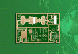
RF (radio-frequency) PCBs and microwave PCBs manage signals at higher-than-audio frequencies and can be found in many of our everyday devices like laptops, smartphones, tablets, and wireless routers. The specialized components on these circuit boards handle RF-specific tasks like signal generation, amplification, and frequency conversion. Integrating RF and non-RF components on the same PCB helps to shorten signal paths and reduce sources of noise or interference.
The RF components in these circuits require a very specific material that meets high-frequency performance requirements. These materials must have a low loss and tightly controlled dielectric constant, as well as be stable over a wide operating temperature range. These factors drive the choice of substrate materials for RF circuits, which can include popular FR-4 base substrates, specialized RF material with lower dielectric losses and higher dielectric constant, or other advanced metallized ceramics.
These specialized materials allow the rf pcb design to operate reliably over a broad range of operating conditions and provide excellent electrical performance with minimal signal loss. These characteristics are vital to ensuring that RF-specific functions like signal amplification and transmission are effective, and that they do not degrade or interfere with other components in the system.
How RF PCB Design Contributes to Improved Manufacturability
In addition, RF PCBs must be able to withstand a high level of electromagnetic radiation and ensure that the RF components are shielded from external sources of interference. These features make RF PCBs more complex than their non-RF counterparts. However, these issues can be avoided through design optimization, careful selection of components and materials, and meticulous layout of the traces and components on the board.
RF PCB design can be challenging due to the many factors that influence performance, including impedance matching and RF signal isolation. The first step is to choose the right PCB material, which must be stable at high-frequency operation and have a low loss tangent to avoid signal degradation. The second step is to select the correct characteristic impedance value, which determines how much power is lost when the RF signal travels along the PCB.
The next step is to plan the component placement based on the function of each component and the connections required by other components. Ideally, the RF components and traces are located on the top layer, followed by a ground plane and power plane. This layout helps to isolate RF and non-RF components to reduce the risk of interference between them.
During the manufacturing process, automated inspection and X-ray testing are used to detect any defects in the PCB material or solder joints that could negatively impact the RF circuit’s functionality. Tests such as network analysis to measure S-parameters and time-domain reflectometry are also conducted to evaluate the RF circuit’s performance.
Finally, a thorough quality control inspection is conducted to verify that the RF PCB conforms to the manufacturer’s specifications. These tests help to identify potential problems, such as voids in the substrate or solder joints, traces that are too long or too short, and discontinuities or mismatched impedance. These defects must be corrected before the RF circuit board can undergo final assembly and testing.